|
I have several ongoing projects, ranging from THz radio-over-fiber communication and sensing technology,
nano-structured silicon solar cells to attosecond science and technology.
The last of which is a new initiative and I expect to devote considerable time for its execution in the next five years.
Synopses of these ongoing projects are summarized below:
[ 1 ]
Studies of Key Components and Technologies for Radio and Ultra-Wideband
Over Fiber Communication System at V- and Beyond W-bands (Main)
(NSC, Aug. 1, 2009-July 31, 2012)
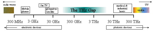
Terahertz (THz) wave, the relatively less explored
electromagnetic radiation in a frequency interval from 0.1 to 10 THz,
has traditionally only been the domain of astronomers and molecular
spectroscopists. Relatively few applications relevant to the society in
general have been explored, however. The so-called THz gap of the
electromagnetic spectrum is illustrated below:
Relatively few applications relevant to the society in general have been explored, however.
Spurred by discovery of new physical principles and innovative technologies in photonics,
advanced materials and nanotechnology, novel applications of THz waves (also called T-rays) in basic science,
security, medical diagnostics and treatment, nondestructive inspection,
and manufacturing quality-control have recently been
demonstrated.
THz sensing, in particular, has attracted lots of attention due to it is molecular unambiguousness.
THz imaging potentially can even allow spotting the onset of cancer and is complementary to widely
used techniques such as optical coherence tomography (OCT).
As a result, companies such as Nikon, Coherent, Picometric and Teraview are pursuing commercialization of THz technology.
Marketing opportunities for security screening in airport,
counterfeit prevention in drugs/pharmaceuticals, defect detection in semiconductor manufacturing,
and other high-value areas appear promising.
Nonetheless, these efforts are hampered for the lack of room-temperature THz emitters or
THz receivers that cost just a few dollars and are the size of a coin.
Information and communications technology should also benefit from advances in THz science and technology.
The synergy of research areas such as wireless communication,
biomedical and environmental sensing, as well fiber-optic
communication with THz science and technology will generate a wealth
of applications in, for example, biometrics — the development of
recognition techniques based on unique human physical or behavioral
traits — using a THz camera, massive sensor networks and selective
communication. Taiwan
is actively pursuing Wimax technology (2-11 GHz), while a Wireless HD (WiHD) Interest
Group (http://www.wirelesshd.org/)
was recently established by companies like NEC, Sony, Samsung and
LG. Its goal is to establish a wireless digital interface to combine
uncompressed high-definition video, multichannel audio data toward
the unlicensed 60 GHz band.
Extending wireless communication to the THz frequency band is one of the holy grails for researchers in THz science and technology.
A roadmap of THz Science and Technology in information and Communication technology was recently put forward by Tonouchi [Nature Photonics, 1(2):97, 2007]:
A roadmp of THz Science and Technology in Information Technology
Recently we have made significant breakthroughs in THz communication and sensing, e.g.,
the demonstration of directly modulated THz audio and burst communication link and integrated THz biosensing chip.
This is possible only through emergence of novel THz functional elements such Photonic THz transmitters and liquid crystal tunable
THz photonic devices developed by the PIs. In this project,
we propose to demonstrate certain milestones of ultra-wide-band (UWB) THz impulse radio communication and sensing
network for future ultra-broadband media, data and biomedical applications using the discoveries mentioned above.
For the near-term (five to 10 years), however, it is more practical
to consider a V-band or W-band ROF or ultrawide band over fiber (UOF)
system.
The broadband data signals are first transmitted in an optical fiber
that has low propagation loss and high data capacity. Then, the
signal is radiated in free space over the last mile to the end user
via a photonic transmitter. The system can thus provide broadband
wireless communication services for the user.
The figure below shows the conceptual setup of the radio-over-fiber communication system and its key components.
By using such system, we can distribute the W-band optical signal through the nearly lossless optical fiber and radiate
it for the end users. Hence, the problem of huge free-space propagation loss of W-band signal can be minimized.
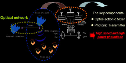
The proposed Radio-Over-Fiber Communication system and its key components
This project is an integrated project joining the efforts of teams
from NTHU, NCU, and NCTU. We will develop the key components and
related technology, including the optical sources, active
components, and high-speed circuits for the applications
radio-over-fiber (ROF) and ultra-wideband (UWB)-over-fiber (UOF)
communication systems at V- and beyond W-bands. We will also
integrate the developed components by use of flip-chip bonding
technology and test the transmission characteristics, which include
eye-patterns, bit-error-rate, and error-vector-magnitude, of such
integrated module. Regarding the optical sources for ROF
communication system, a clean and continuous-wave (CW) optical MMW
sources with over 100GHz operating frequency will be demonstrated.
On the other hand, the shaped optical pulse trains with special
coding scheme, whose envelop cover all the available W-bands
(75-110GHz), with high repetition rate (>10GHz) will also be
developed for the applications of UOF system. In order to convert
the high-power optical signals from UOF or ROF central stations, we
will also demonstrate novel high-power photodiodes with over
(120GHz) bandwidth and high saturation current performance (20mA).
Furthermore, in order to further amplify the radiated CW or peak
power and reduce their phase noise, we will also demonstrate some
novel nonlinear circuits, such as GaN based piezoelectric oscillator
at W-band, injection-locked oscillator array, and novel
printed-circuit antenna array with high directivity (~20dB) at V-
and W-bands. Nitride-based quantum cascade structures can
potentially be developed as room-temperature THz laser devices.
Overall, this project will cover key active/passive devices,
circuits, optical sources, and the test beds for ROF and UOF
communication system at V- and beyond the W-bands.
[ 2 ]
Photovoltaic technology with self-assembled nanostructures of silicon quantum-dots in mesoporous
silica (NSC Nanoscience Program, Aug. 1, 2008- July 31, 2011).
The project team consists of Prof. C. T. Lee (NCKU), who acts as PI
of the whole project, and members from NCTU and NDL. I am
responsible for overseeing the NCTU (Profs. Jung Y. Huang, Ci-Ling
Pan, Hao-Chung Kuo, Peichen Yu and Hyeyoung Ah) and NDL (Dr. Jia-Min
Shieh) portions of the project and also lead the effort on
investigating the underlying physical mechanisms in the novel
nanostructured silicon material. Experimentally, various ultrafast
and THz spectroscopic techniques will be employed, in additional to
the more conventional spectroscopic methods, such as spectroscopic
ellipsometry. Previously, enhanced UV-to-NIR photoresponse has been
reported by the NCTU and NDL team for a photodiode with dense
silicon quantum-dots embedded in MS. Phototransistor-like operation
due to enhanced exciton resonant tunneling and injection was
observed. We thus propose a related solar cell structure made of a
superlattice of silicon quantum dots with gradually varying sizes
inserted between p- and n-type tailored mesoporous materials. To
enhance the PV efficiency, various approaches involving
cost-effective methods for transmission enhancement of solar energy
will be investigated. For example, a double-layer anti-reflective
structure consisting of a dielectric film and a mesoporous layer of
low refractive index will render the front surface of the device
more effective in capturing photons. Preliminary results confirm the
validity of this approach. Further, Indium-Tin Oxide (ITO)
nanostructures not only offer broad angular and spectral
anti-reflective characteristics, but also improve the electric
properties of the cell, reducing the screen ratio of metal contacts.
Initial work is promising (Adv. Mat., 2009). Moreover,
surface plasmonic effects using periodic and random metal nano-particles
can be designed to enhance the transmission in the vicinity of
bandgap energy. Finally, it has been suggested that silicon nano-pillar
structures can significantly alter the thermoelectric properties of
bulk material. Hence, we will explore nanostructures with a high
thermoelectric coefficient in order to harvest the waste heat from
p-n junctions. In addition, a surface plasmonic coupling layer or
even an optical antenna structure can be employed to offer
free-space-to-device photon-capturing functionality without coupling
loss. Finally, a wavelength up-conversion layer can be realized with
appropriate nanocrystals embedded in MS to convert solar radiation
from near IR to the visible region, promising efficient use of
photons over the entire range of AM1 solar spectrum.
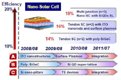
ResearchRoadmap for highly efficient nano-silcon solarcells
[ 3 ]
Towards Tabletop Sub-Single-Cycle Attosecond Laser Sources (NSC, August 1. 2009-July 31, 2012)
Attosecond (1 as = 10-18
sec) science is generally recognized as one of the frontier areas in
science today. There are many potential applications. For example,
Few cycle attosecond pulses have been used to create and then probe
interference of vibrational wave functions in a molecule; control a
simple chemical reaction [4] and to enable real-time observation of
electron tunneling in atoms. The shortest pulse that have been
generated to date is about 80 attosecond.
In this work, we propose a new scheme of sub-femtoseocond (attosecond)
pulse generation by starting from a single nanosecond laser and
phase lock the cascaded harmonics generated by second-order
nonlinear optical processes. It is shown that sub-cycle attosecond
pulses with carrier envelope phase (CEP) control can be generated in
this manner. After full characterization such a light source will be
used to study the generation of higher-order harmonics (HHG) with
extreme ultraviolet (XUV) emission by half-cycle attosecond optical
pulse and the generation of even shorter attosecond pulses. Such
broad ultrashort pulses, spanning a spectrum from the near infrared
to the XUV would be invaluable for dynamic studies of the condensed
matter, including biomolecules. The availability of this source
should stimulate both theoretical and experimental studies of
light-matter interaction on the attosecond time scale. Our vision
of attosecond science and technology is shown in the figure below.
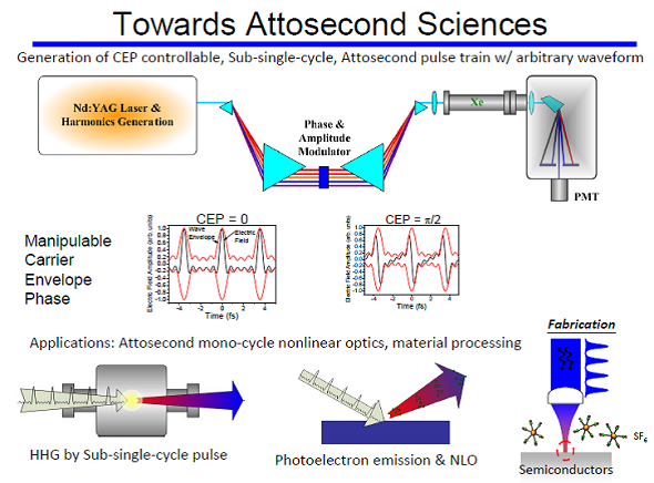
A vision of attosecond science and technology
We have successfully completely the first phase of the construction
of the Tsing Hua Attosecond Source. As a first demonstration,
saw-tooth and square waveforms were synthesized. Initial results
were presented at FiO2010.
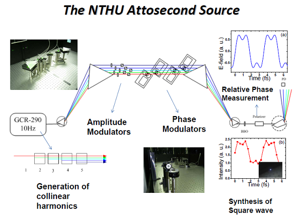
The Tsing Hua Attosecond Source (Phase one)
[ 4 ]
Industrial Collaborations:
There are two on-going projects:
In collaboration with CW Laser Corportation, we
propose to improve the performance of traditional small form-factor
diode-pumped and frequency-doubled solid-state green laser. The key
task is the stabilization of the operation wavelength of the diode
pump laser. Various approaches for wavelength locking will be
explored. The operation temperature range of this laser is expected
to extend from 0 to 50°C. Such lasers will be much more suitable for
industrial applications such as instrumentation in outdoor
environments and the laser display.
In collaboration with Prime Optical Fiber Corporation (POFC) and the
CW Laser Corporation, we have been conducting research and
development of advanced short-pulse fiber-based lasers. By
frequency-doubling technique, we will also demonstrate high power
green output. Such lasers would have immediate applications in
scientific research, laser-based manufacturing, laser display and
biomediciene. The tasks for the first year consist of the design,
construction and optimization of mode-locked Yb-doped fiber lasers
with average power > 5 Watts and pulse width <1ps. We also expect to
generate green output exceeding 3 Watts by frequency doubling using
efficient nonlinear crystals.
潘犀靈教授實驗室(Ci-Ling Pan Laboratory)
進行中的主要的研究計畫
[ 1 ]
兆赫光子科技: V和W頻段無線與超寬頻訊號光纖通訊之關鍵元件及技術之研究-總計畫暨子計畫一:
超寬頻訊號載於光纖通訊之基礎與應用研究(國科會NSC, Aug. 1, 2009-July 31, 2012)
兆赫輻射(Terahertz Radiation, 1 THz = 1012 Hz)
是頻率從十分之一兆赫到十兆赫範圍內的電磁波的簡稱。相對於X射線,兆赫輻射也被稱爲T射線,
其波長在次毫米波範圍30到300微米),屬於遠紅外線範疇。
這一頻率範圍內的電磁波的相關研究具有豐富的科學內涵和廣泛的應用前景:
如遙測、顯像與通訊等。最近我們在這方面有重要的發現與突破,如實現了各種結合液晶、
光子晶體及meta-material結構之可操控THz光電元件、次毫米波的光電式發射器及雛形聲訊兆赫連結等。
將無線通訊拓展至兆赫波段長久以來都是兆赫科技研究的聖杯,THz科技在資通領域之Roadmap請參考下圖
(取自 M.Tonouchi, Nature Photonics, 1(2):97, 2007):
NTT利用UTC-PDs>已證實120-GHz-band millimetre-wave wireless links的可行性,
預期2015年可提升至100G bit s-1。在這同時,混成式的無線電-光纖通訊越來越受到矚目。
60GHz無線電-光纖通訊網路即將商品化。我們組成由中央大學、清華大學、交通大學研究群的團隊,
開始探討在W-band及更高頻段(> 100 GHz)的超寬頻突波無線-光纖通訊的若干重要議題:
- 超過W-band的光電式厘米波發射器及其關鍵元件:高功率/高效率光偵測器的測試。
- 建立1550 nm-based UWB-IR 超寬頻脈碼無線-光纖通訊測試平台。
- 展示1550 nm-based之10 Gb/s UWB-IR 無線-光纖通訊連結及加碼與解碼技術。
[ 2 ]
高效率矽奈米結構太陽能電池:含自組裝矽量子點之奈米孔洞氧化矽複合材料之光伏特技(國科會NSC, Aug. 1, 2009-July 31, 2012)
太陽能技術在科學上必須有革命性之突破才能於2030年達到累積光伏特產品4TW,模組單價低於0.3 $/Wp之目標。
本課題畫提出一新型太陽能電池結構,其主要結構為一埋藏於n型或p型奈米孔洞氧化矽材料內之尺寸漸變矽量子點超晶格,
並採用各種方案,如雙層抗反射結構或以氧化銦錫(ITO)奈米柱狀結構層,以更有效以增強太陽光之穿透效率並提昇捕捉光子之能力。
應用表面電漿的耦合結構,我們預期將可進一步達成自由空間至元件內部的無損失光耦合功能。
最後,利用高熱電特性的矽奈米柱製作熱電轉換元件,充分利用操作時所散發出的熱能並維持元件在最佳的溫度工作,
我們期待孕育高效率(15%)低價位之光伏特技術。在本課題中,我們將整合理論與實驗研究,
以第一原理及自由度N成一次方關係之高效率數值模型,
來暸解與優化矽碳-矽-矽鍺薄膜系統及含自組裝矽量子點之奈米孔洞氧化矽複合材料之電子結構與傳輸效應,
並將利用密度泛函理論為基礎之緊密鍵結模型加以評估整體載子之傳輸特性。
上述新穎材料的載子傳輸特性可以非接觸的方式,利用超快與兆赫同調光譜技術量測而加以驗證。
這個計畫整合國立成功大學,國立交通大學,國家奈米元件實驗室及國內數家廠商,是進行中的奈米國家型科技計畫學術卓越計畫。
高效率矽奈米結構太陽能電池研究藍圖Roadmap
[ 3 ]
新型寬頻次飛秒光源產生與光同調性研究:桌上型亞週期阿秒雷射光源之研究(國科會NSC, Aug. 1, 2009-July 31, 2012)
單週期(single-cycle,亦即阿秒與兆赫波)光子學是目前光電科學的前沿領域。
目前,由兆赫至軟X-射線的單週期電磁波已被實現。由如此先進光源發射的光波的各種特性都能準確控制。
掌握如此威力強大的工具,科學家們得以前所未有的清晰度鉅細靡遺的研究。
潘教授在超快及兆赫科技領域已研究多年,在本計畫中,我們提議一種新的方法來產生次飛秒(阿秒尺度)的光脈衝:
以一具高能量的奈秒級雷射,利用非線性晶體中的二階非線性效應,各級串接的方式產生雷射基頻的二、三、四及五次諧波,
並加以相位鎖定及控制,則其合成之光脈衝將短至次飛秒級,且其脈衝包絡相位(carrier envelope phase)可控制。
經由高階諧波產生(Higher Harmonic Generation),預期應可在短期內產生短至XUV(~ 50nm)波長的同調光。
下圖是我們從事阿秒科技研究的構想與藍圖:
最近,此新型阿秒(attosecond, 1 as = 10-18秒)雷射系統的雛形已由潘教授的團隊在清華大學架設完成。
作為初步的驗證,我們用三個諧波合成方波與鋸齒波,量測與理論預測相符,初步結果已發表於2010年FiO。
清華阿秒光源
我們正針對此光源作完整的特性檢測與分析。同時,我們試圖以此亞週期阿秒光源產生高階諧波。
這將是首度用亞週期光脈衝進行的類似實驗,因此其結果將眾所矚目。
控制低階與高階諧波的振幅與相位,我們將有機會產生較目前各種提議的方法更小一個數量級的阿秒超快光脈衝
頻譜涵蓋近紅外、可見光與極紫外或軟射線波段,適合凝態物質,包括生物材料的研究。
[ 4 ]
產學合作
(a) 應用於雷射精密加工之高尖峰功率光纖雷射之研發(虹竣科技、卓越光纖、國科會NSC, Sept. 1, 2010 - Aug. 31, 2013)
材料與工件處理是雷ㄑ射產業最重要的應用之一,我國的雷射加工產業最近蓬勃發展,
最近固態照明與太陽能電池產業對高速晶片切劃(lase wafer scribing)的需求殷切,而雷射加工機的關鍵組件:
雷射光源仍多由國外進口。目前,晶片劃片目前多採用紫外光雷射(355nm 與266nm)。
與虹竣科技、卓越光纖POFC 合作,我們提議研發先進的短脈衝、高功率Yb 光纖雷射,再經由非線性頻率轉換技術將之轉換至紫外光,以應用於雷射加工之用。
光纖雷射規格分年達到平均功率 <10W, 尖峰功率 >10KW, 雷射脈寬 < 10 ps(第一年);平均功率 >20W, 尖峰功率 >100 KW,
雷射脈寬 < 2 ps(第二年);平均功率 >50W, 尖峰功率 >250 KW, 雷射脈寬 < 1 ps(第三年);
倍頻與四倍頻效率分別達50%與20%。我們亦將探討直接利用皮秒及次皮秒等級的近紅外雷射加工,如劃片的可行性。
(b) Light Peak 技術用新穎光纖之研究(卓越光纖、科學工業園區研發精進產學合作計畫,Oct. 1, 2010 – Sept. 30, 2011)
市場上,光纖的應用正快速的由通訊擴大到電子產業,進入最重要也是銅質纜線力守的使用者端之電腦及消費性產品領域,
為了及早掌握這個市場發展契機,本公司將以多年來,在開發光纖預型體、光纖絲以及光纜等產品,所累積的深厚技術為基礎,提出本項計畫;
本計畫的目標在於完成開發一種全新的、能夠滿足應用於Light Peak及類似應用產品特性的專用高強度、耐彎曲多模光纖與光纜產品,
並建立相關產品端性能驗證測試設備、標準與流程。主要的產品開發工作由卓越光纖公司負責完成,其中分為四項目標;第一、大纖(80um)
低損失光纖預型體與GGP光纖抽絲製程開發,第二、低折射率層材料與結構的開發,第三、滿足應用850nm雷射波長時
,達到高頻寬之光纖材料開發,第四、發展高機械強度、高可繞性光纖絲與纜線之製程技術。
本計畫目標光纖產品則委託潘犀靈教授帶領之研發團隊,開發一套高效率的產品端性能驗證測試標準與流程,
以作為未來本目標光纖產品量產時之品質檢測標準。
|