實驗室概況:
(I) 先進奈米薄膜製程實驗室
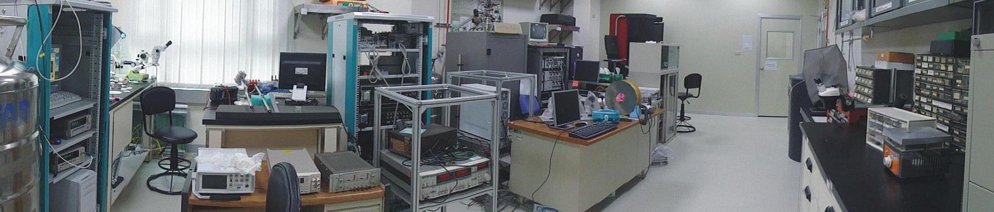
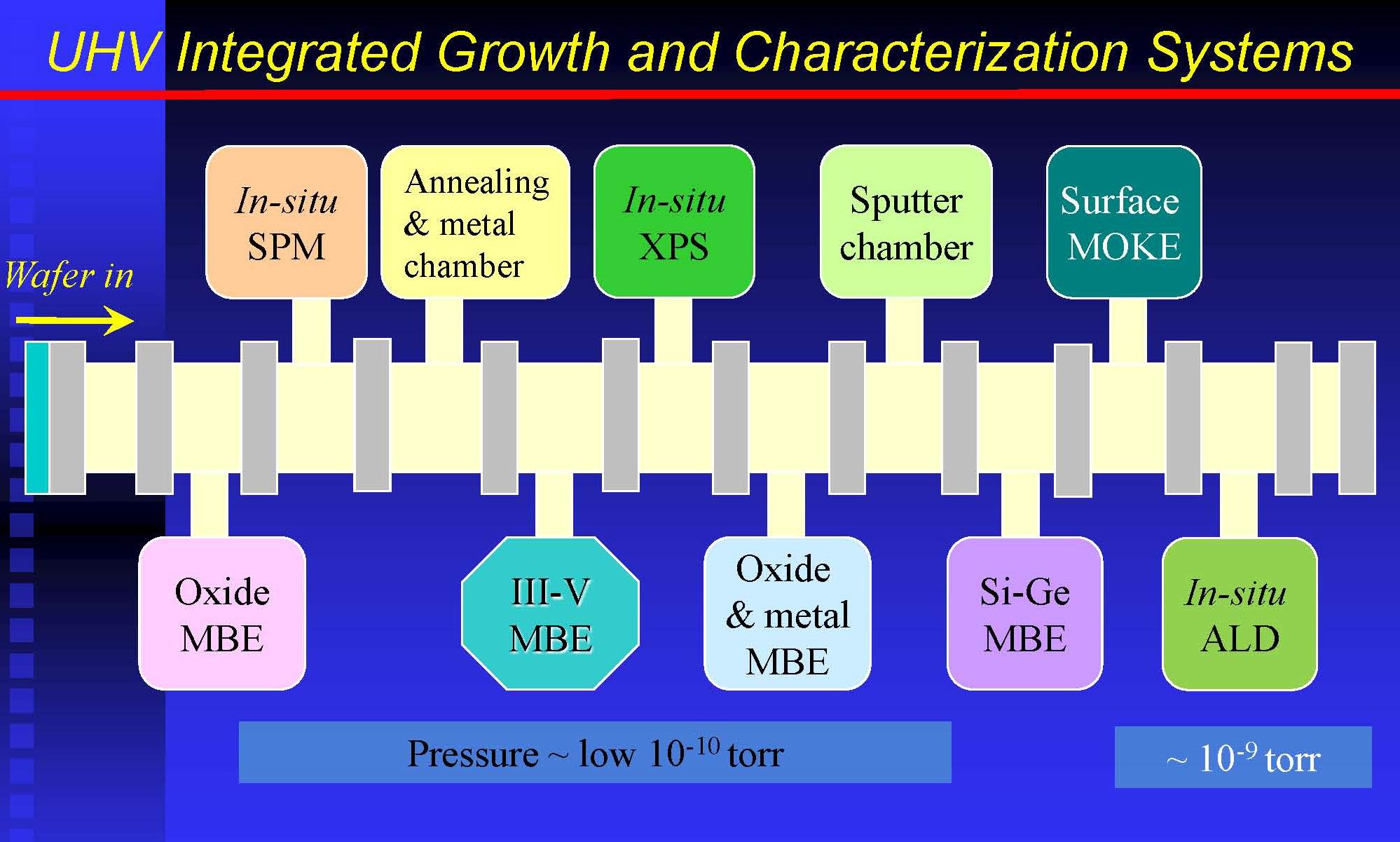
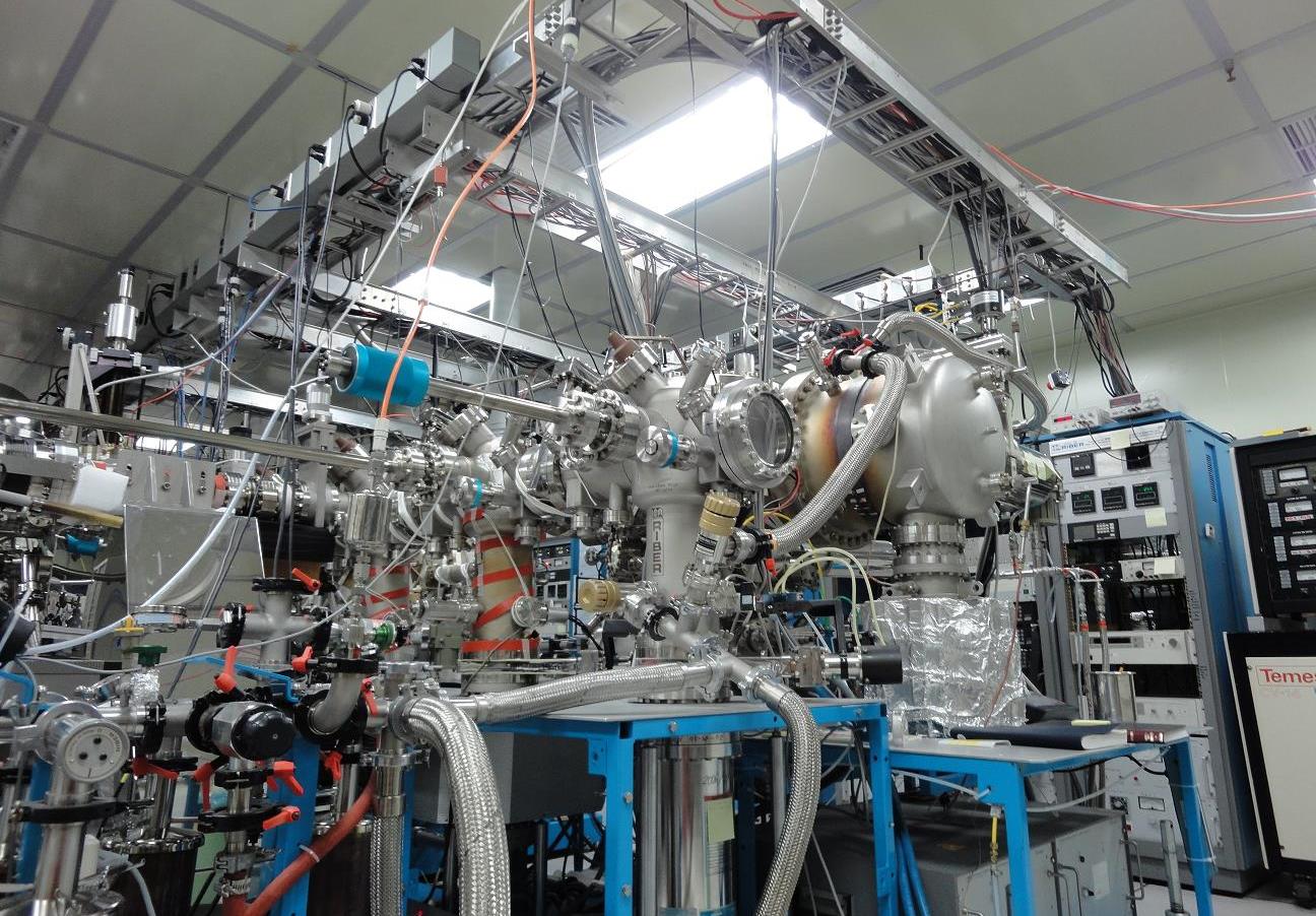
實驗室位於工研院奈米中心(67館) 下為實驗室簡圖
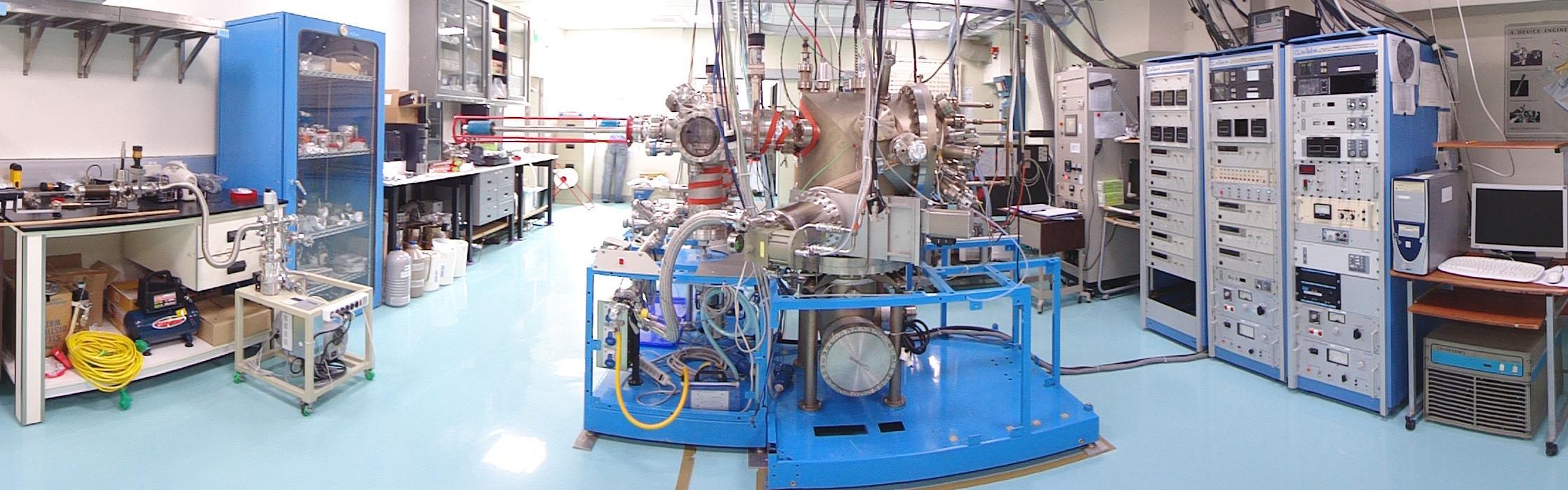
A.140室 : 分子束磊晶多腔超真空系統實驗室(MBE-multichamber UHV system Lab)
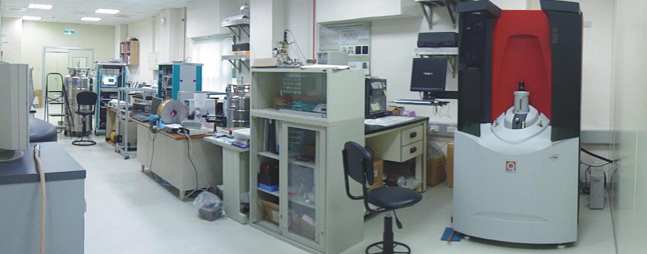
B.145室 : 薄膜製程與量測實驗室(Thin Film Processing and Characterication Lab)
(I) Advanced Nano Thin Film Epitaxy Lab
The Lab is located in ITRI NanoTechnology Research center (building 67).
This is the sketch of our lab:
A. Room 140 : MBE-multichamber UHV system Lab
B. Room 145 : Thin Film Processing and Characterication Lab
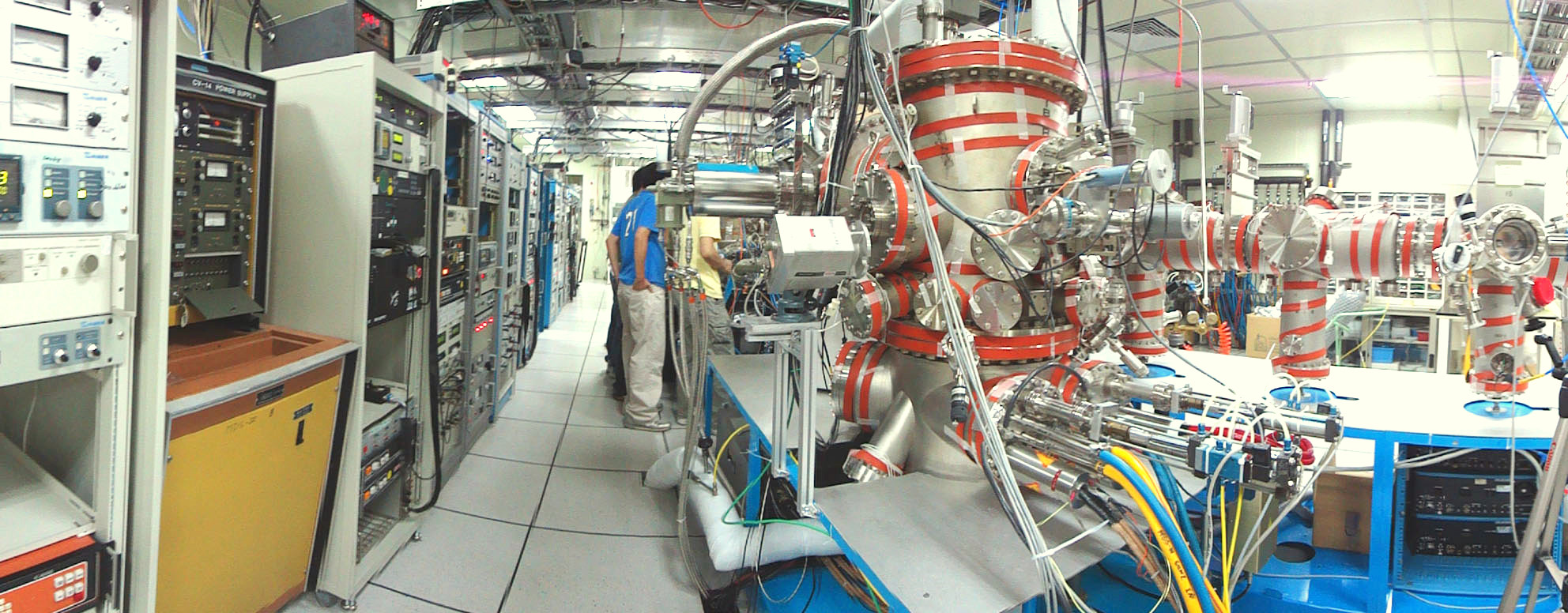
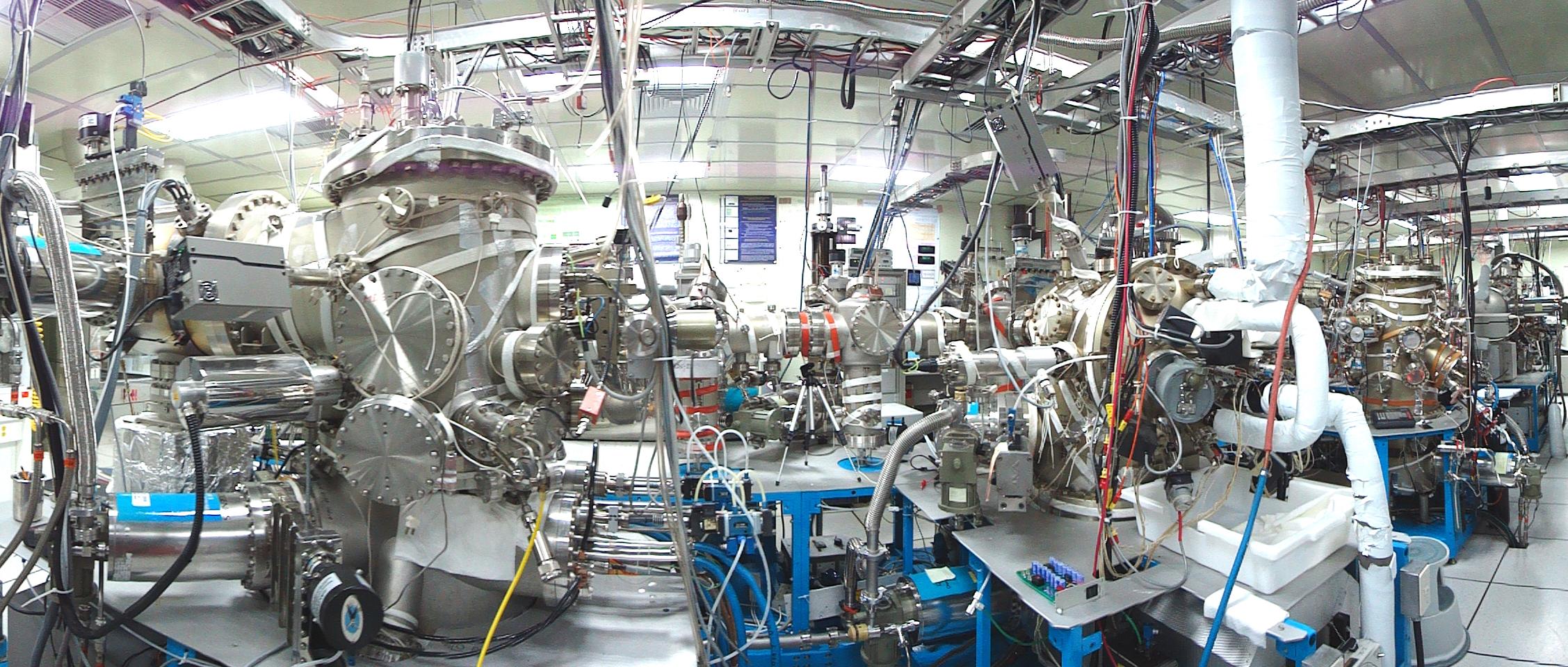
圖片左方為電源供應器和一些電子控制儀器,右方依序為成長矽-鍺,成長氧化物和金屬在III-V族材料上,III-V族半導體,及在矽上成長高介電常數的介電層的各種分子束磊晶系統 。
The power supplies and electronics racks are located at the left-hand side, and Si-Ge , Oxide & Metal for III-V , III-V MBE, and High k dielectrics for Si chambers are located at the right-hand side.
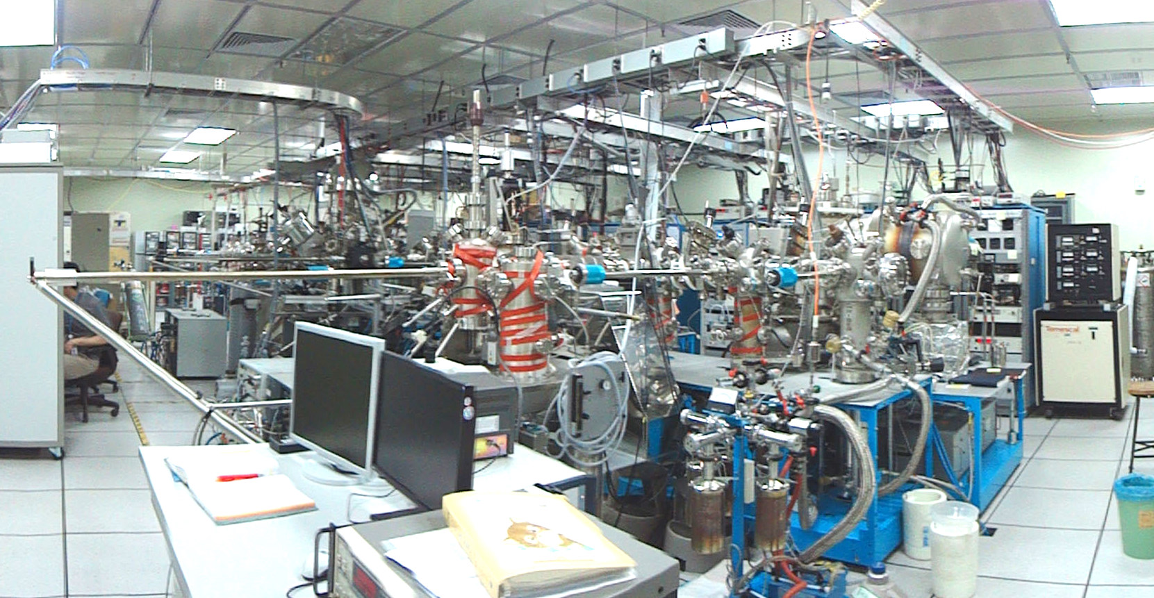
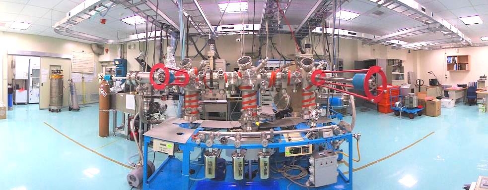
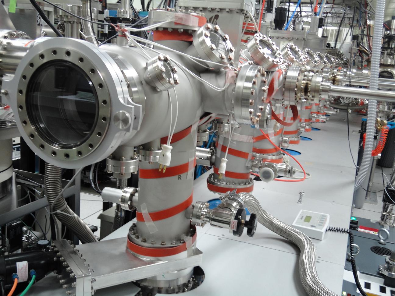
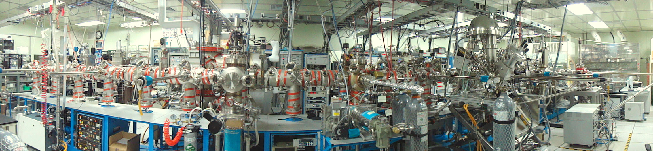
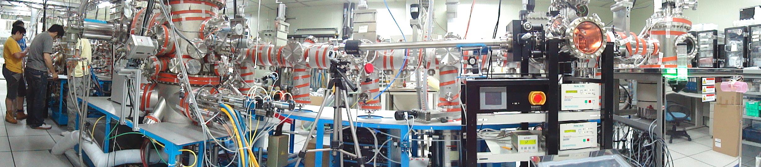
由一chamber移至另一chambe
In-situ UHV transfer modules
Sample Load Lock End
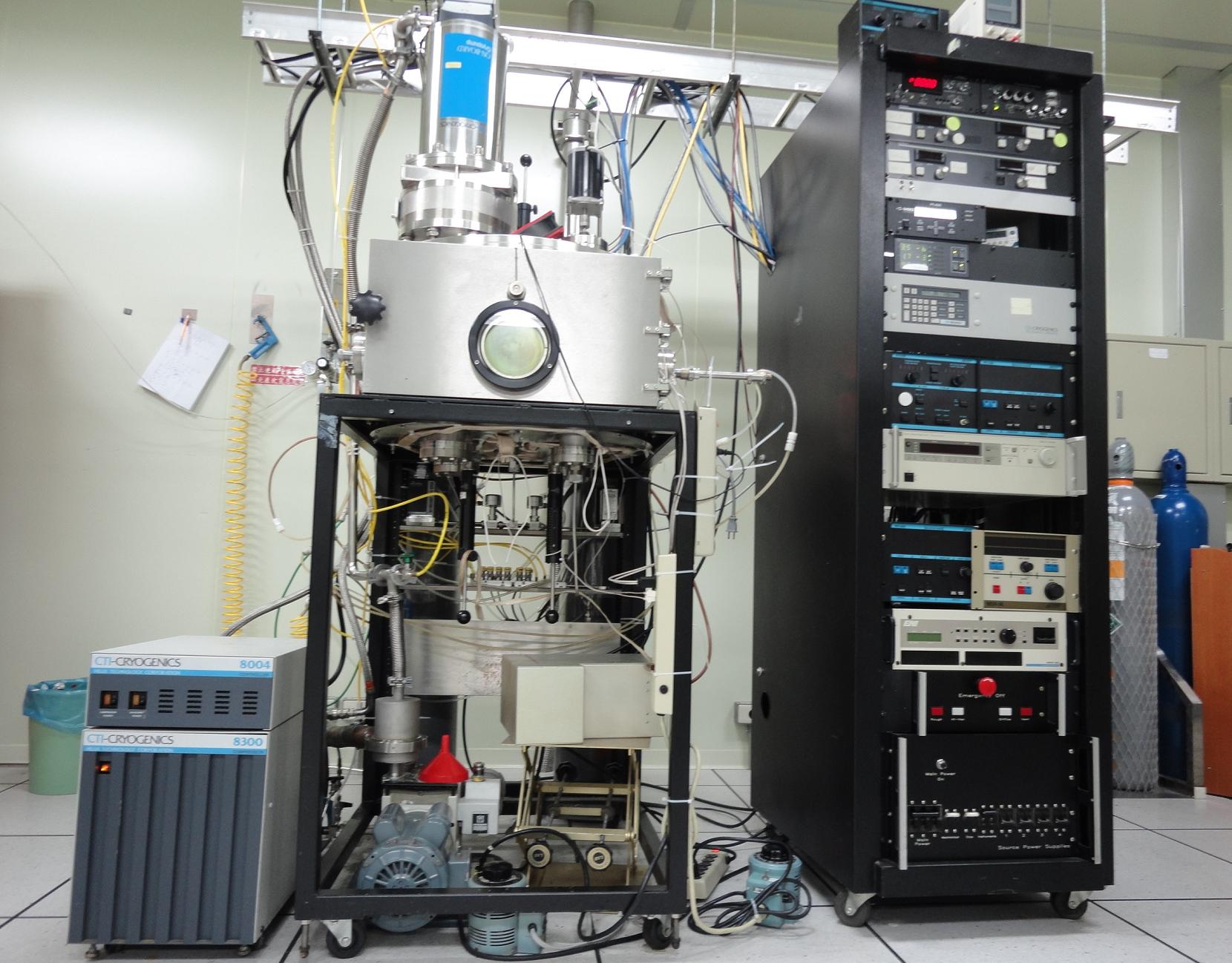
分子束磊晶系統 MBE SYSTEM
分子束磊晶(MBE)為一精密的真空蒸發系統,在1975年由 Cho and Arthur發展出來的儀器.它的主要優勢是可以控制MBE成長異質結構到一個分子層的尺度,這是因為我們可以精準的控制它的成長速率在一很低的值以下(約每秒1分子層)經由控制各不同元素的shutter我們可成長各不同元素的陡峭介面。
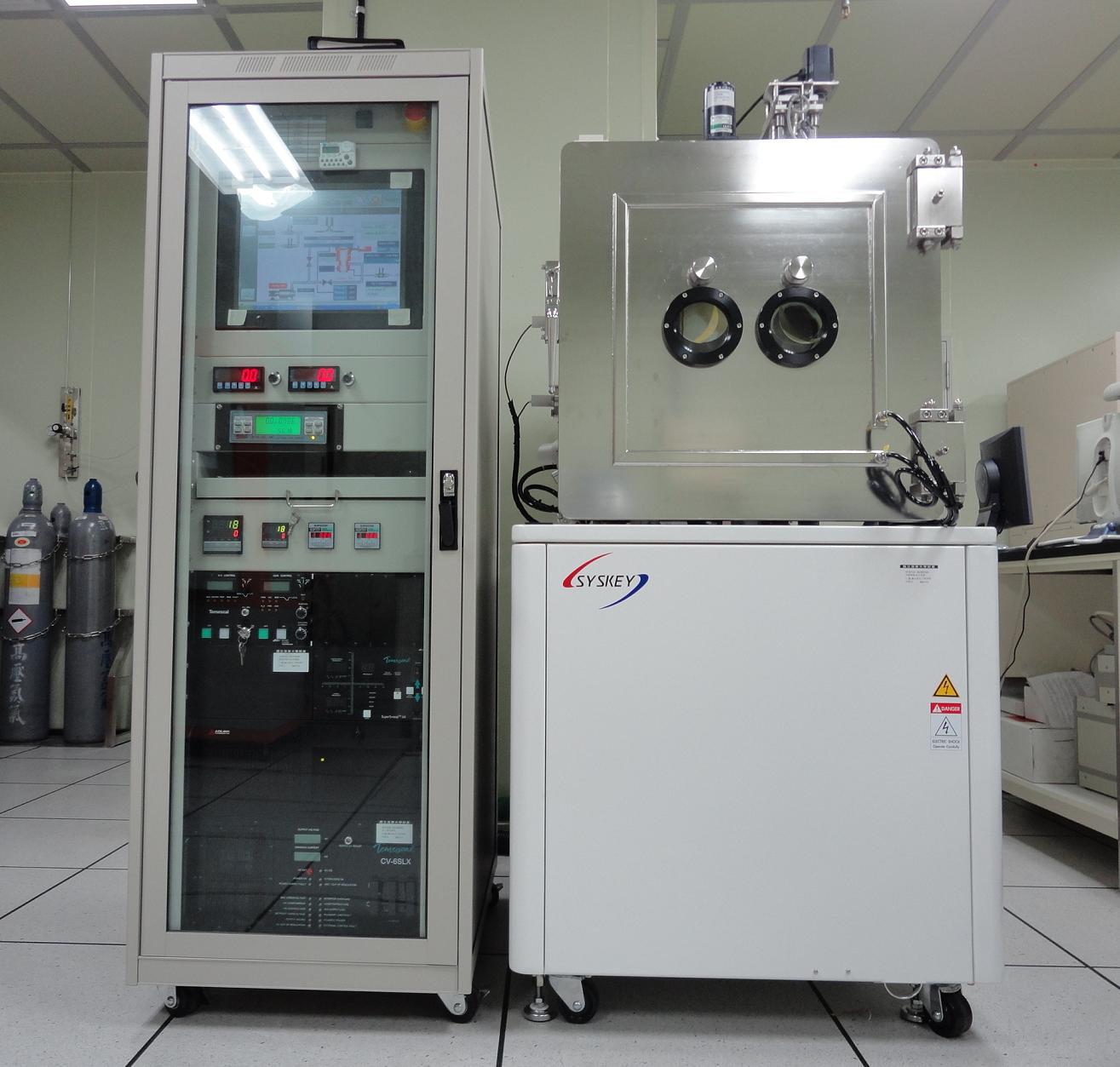
濺鍍機
Sputtering System
濺鍍為一最常用的沉積薄膜方法.因為它只牽涉到簡易的物理過程,它較富有彈性,可依不同的需求做出調整.因此它被廣泛的應用於半導體和光電上。濺鍍機的特性是可在鍍膜時調整不同化學成分與成長不同結構的薄膜。
Sputtering is one of the most commonly used methods for the deposition of thin films. Because of its simplicity the physical processes involved, versatility of the technique, and flexibility for alteration and customization, it is widely used in the materials research. The nature of the process of sputtering makes available ions that can be utilized for tailoring the chemistry or the structure of the film.
電子束與熱阻絲蒸鍍系統
Electron beam and thermal evaporation system
電子束蒸鍍與熱蒸鍍為鍍金屬膜中很普遍的方法,顧名思義,電子束蒸鍍即是利用高壓電子束直接轟擊放置於坩鍋內之材料,如常用的鋁、鈦、鎳、金、鉑等,使其分離出來沉積於目標基材上,大部分的金屬皆可利用此方法來蒸鍍。而熱蒸鍍則是利用鎢舟加熱所要蒸鍍之材料,如金、鈀等,到達其沸點後開始鍍膜。
Electron beam and thermal evaporation systems are broadly used for metal deposition. By introducing a high voltage electron beam to the sources, metals like Al, Ti, Ni, Au, etc, can then be evaporated to the substrate. Thermal evaporation is conducted by heating a tungsten boat to the boiling point to evaporate the metal sources like Au, Pd, etc.
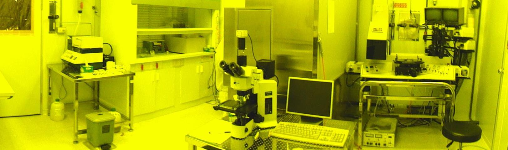
黃光室
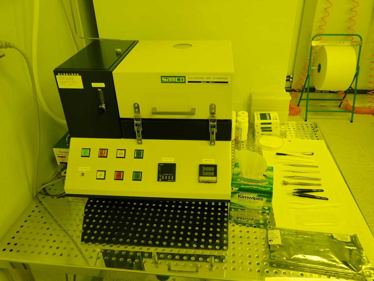
紫外光臭氧清潔機是利用在加熱的環境下,紫外光跟臭氧的作用,來達到去除基材上的有機物,如光阻等。
UV-OZONE stripper/cleaner uses a unique combination of ultraviolet radiation, ozone, and heat to gently, yet effectively, remove organic materials from substrates.
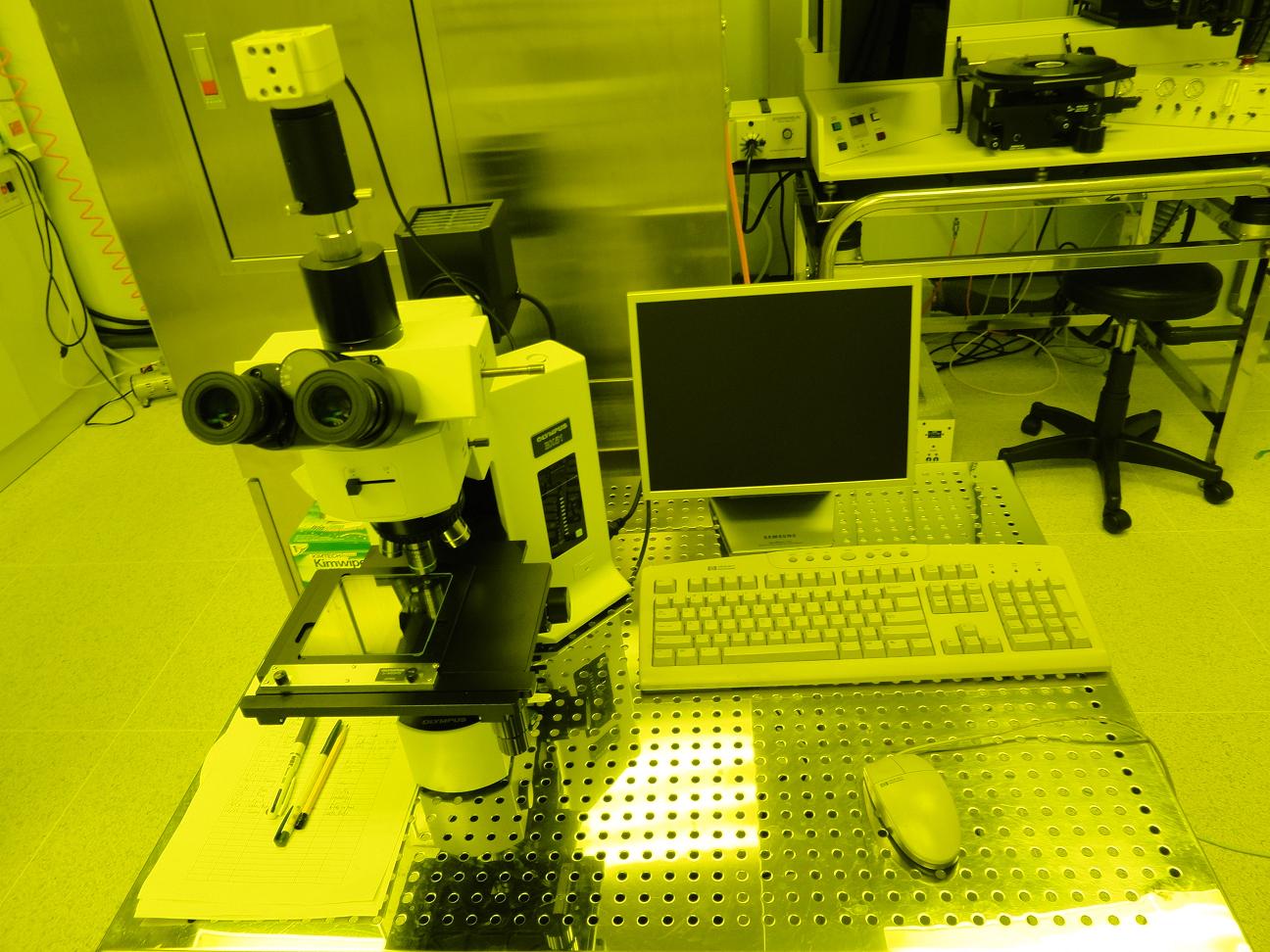
光學顯微鏡,具備上下光源明暗視野功能,十倍目鏡搭配五至一百倍之物鏡,最大放大倍率為一千倍。
Optical Microscope with incident bright field/dark field illumination tube and microscope frame for transmitted and reflected light microscopy. Wide field eyepiece of 10X plus objective ranging from 5X to 100X, giving a max 1000X in amplification.
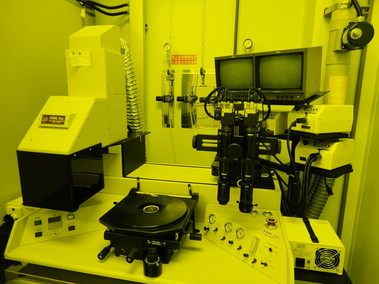
ABM接觸式光罩對準曝光機為黃光微影製程用,藉由500瓦之(深)紫外光光源,搭配濾鏡控制之365/405奈米波長,曝照光阻以達到於試片上製造圖樣的效果,曝光顯影出之線寬可達0.5微米。
ABM contact mask aligner and exposure system, featuring a 500 Watt DUV/NUV Light source with inclusive mirror sets for 365/405 nm wavelength, is used for photo resist patterning down to 0.5μm in spacing.
實驗室位於清華大學物理館205室
物理性質量測系統 (Physical Property Measurement System ,PPMS)
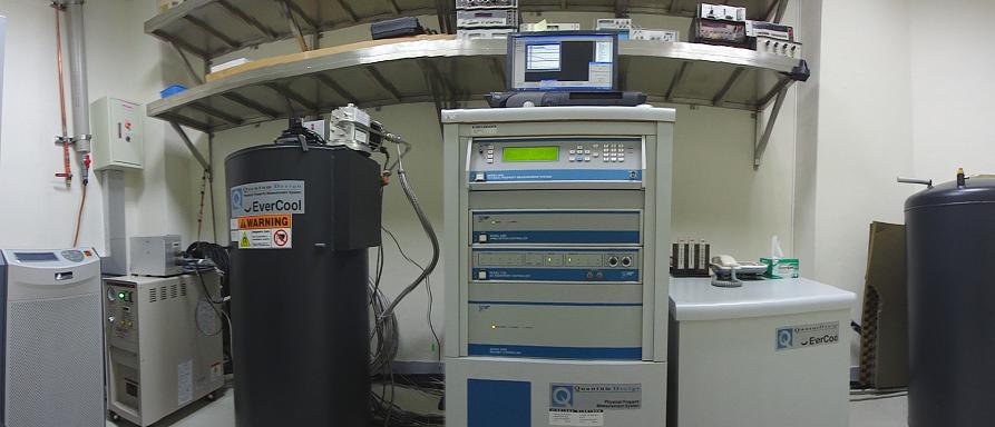
物理性質量測系統是一台可以在控制溫度加磁場的情況下量測電信的儀器,其優點在於本身可冷凝氦氣而形成液態氦的功能,減少液態氦損耗,並可自行生產維持液態氦的存量。
Physical property measurement system (PPMS) is a convenient instrument which can measure electric signal under controllable temperature and applied magnetic field. The advantage of PPMS is due to the function of ever cool dewar, which can liquefy He gas and produce Liquefied He (LHe). Hence the consumption of LHe is saved and the storage of the LHe is maintained.